


Samsung Electronics has announced the creation of a new organization within its Semiconductor (DS) Division to oversee end-to-end development of memory semiconductors, including DRAM and NAND flash. The company will also establish a new “Digital Twin Center” to support its plans for an AI-driven manufacturing environment. As part of the restructuring, the HBM (high-bandwidth memory) development team—set up as a separate unit last year—will be integrated into the DRAM Development Division, reflecting confidence that Samsung’s HBM technology has now reached a stable and mature stage.
On the 27th, Samsung Electronics announced the details of the reorganization during an executive briefing. A new “Memory Development Division” will be established under the Memory Business Unit of the DS Division to handle memory semiconductor development. Previously, the Memory Business Unit operated through department-level units such as the DRAM Development Division and Flash Development Division. The new organization will serve as a control tower overseeing all memory semiconductor development. Hwang Sang-jun, head of the DRAM Development Division (vice president), who led the HBM redesign, will lead this organization. A semiconductor industry insider said, “This appears to be a move to establish a control tower to respond to increasingly complex and intense memory technology competition, particularly centered on HBM.”
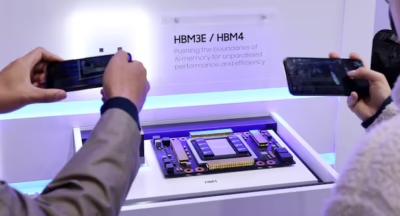
The HBM development team, formed in July last year, will be relocated to the design team under the DRAM Development Division as part of this reorganization. This restructuring aims to concentrate personnel related to HBM development, which was previously organized separately to reclaim technological leadership from SK Hynix. Recent evaluations suggest the reorganization reflects confidence in Samsung’s technological capabilities, as the company has officially confirmed its supply of 5th-generation HBM (HBM3E) to NVIDIA. It was reported that Son Young-soo, vice president who previously led the HBM development team, has been appointed as the head of the design team.
Under the Global Manufacturing & Infrastructure Division of the DS Division, a Digital Twin Center will be newly established. A digital twin is a virtual environment that replicates real-world spaces and operations. Last month, Samsung Electronics announced plans to build an “AI factory” by applying AI to all semiconductor design and production processes, after securing 50,000 graphics processing units (GPUs) from NVIDIA. The company stated it would implement a digital twin manufacturing environment based on NVIDIA’s simulation platform, Omniverse. Analysis suggests the new organization will focus on research and development (R&D) for this initiative.
The name of the Management Support Division, responsible for the finances of Samsung Electronics and its affiliates, will be changed to “Management Support Division.” This is interpreted as an effort to expand the role of the planning team under the management support organization to discover future new businesses. Samsung Electronics plans to finalize the reorganization within this week and hold a global strategy meeting next month to review next year’s business plans.
(This content is sourced from a syndicated feed. The Japan India Manufacturing Journal website assumes no responsibility or liability for its accuracy, completeness, or content.)
COMMENTS