


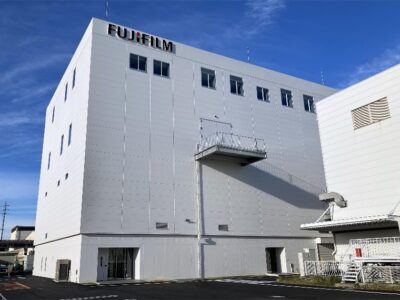
Fujifilm Corporation has completed a new development and evaluation facility at the Shizuoka Factory of FUJIFILM Electronic Materials Co., Ltd. (FFEM), its core semiconductor materials business. The building became operational this month and is designed to accelerate innovation in next-generation semiconductor materials while ensuring a reliable global supply.
The expansion comes at a time when semiconductor demand is rapidly rising due to AI, 5G, IoT, and advanced computing technologies. Fujifilm’s semiconductor materials division has grown significantly—sales have increased around 1.7 times between FY2021 and FY2024. To support this momentum, Fujifilm invested over 100 billion yen in facilities between FY2021–FY2024 and plans to invest another 100 billion yen or more by FY2026.
The new facility includes a high-grade cleanroom equipped with advanced evaluation tools. Fujifilm has integrated AI image recognition to detect microscopic particles with greater accuracy, improving inspection quality and strengthening quality control. A dedicated digital transformation (DX) team will further enhance production processes through AI and digital technologies, boosting product performance, consistency, and supply stability.
The building has been designed for resilience, featuring a seismic isolation structure and elevated cleanroom placement at 12 meters above ground to protect against flooding. The Shizuoka Factory also collaborates closely with Fujifilm’s global R&D and production teams, supporting high-end process development for customers worldwide.
With this upgrade, Fujifilm aims to advance the development of cutting-edge materials such as EUV, ArF, and NIL photoresists, PFAS-free alternatives, and the WAVE CONTROL MOSAIC™ series used in image sensors. It will also strengthen systems for polyimides used in next-generation semiconductor packaging, meeting growing demand driven by AI-centric chips.
According to Fujifilm, this investment positions the company to lead in the rapidly expanding semiconductor materials market, expected to double by 2030. Fujifilm continues to supply a wide portfolio of semiconductor materials globally from front-end photoresists and lithography materials to CMP solutions, thin-film chemicals, polyimides, and high-purity process chemicals.
(This content is sourced from a syndicated feed. The Japan India Manufacturing Journal website assumes no responsibility or liability for its accuracy, completeness, or content.)
COMMENTS