HomeIndustry update

Rigaku Launches Microspot X-ray Diffraction System For Semiconductor Market

New AI tool for improved ergonomics in the workplace
Tata Electronics and Bharat Electronics Join Forces to Accelerate India’s Electronics and Semiconductor Goals
For More Efficient Production: Wikov Relies on the S41 From STUDER

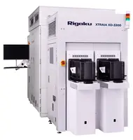
Rigaku Corporation, has recently commenced full-scale commercial production of the XTRAIA XD-3300—its high-resolution microspot X-ray diffraction system.

Amid surging demand for generative AI and data centers, semiconductor scaling and 3D integration are progressing at an unprecedented pace. There is a growing need for next-generation memory solutions like high-bandwidth memory (HBM), 3D DRAM, and advanced logic semiconductors at the 2 nm node and beyond. To achieve the high performance required of these devices, chipmakers are increasingly turning to superlattices—nanoscale integrated structures—based on Si/SiGe (silicon/silicon-germanium) processes. Precise measurement technologies capable of accurately analyzing the composition and thickness of Si/SiGe films have become essential, as they are critical to optimizing device performance and manufacturing yield.

To meet the evolving demands of next-generation semiconductors, Rigaku has developed the XTRAIA XD-3300—an advanced metrology system designed and built entirely in-house, from the X-ray optics to the detector and diffraction software. It stands as the world’s only system capable of performing direct, non-destructive, high-resolution diffraction measurements of superlattice structures on microscopic wafer pads.

At the heart of the XD-3300 is Rigaku’s proprietary X-ray optical system, which combines ultra-high-performance mirrors with bent crystals. This innovation enables measurement speeds up to 100 times faster than previous systems—reducing tasks that once took hours to just a few minutes.

Complementing the hardware, Rigaku’s advanced diffraction software provides highly accurate numerical analysis of superlattice periodicity and interface quality, ensuring precise evaluation of complex multilayer Si/SiGe structures essential for cutting-edge semiconductor performance and yield.

Features of XTRAIA XD-3300

  • Direct visual non-destructive observation of microscopic structures with high-resolution

Provides detailed, non-destructive diffraction of the interiors of nanoscale, multi-layer structures, on fine pads less than 40 µm across. World-top-class resolution feeds directly into improved yield.

  • 100-fold increase in measurement speed compared with previous models
  • Incorporates of the only software capable of analyzing diffraction of complex superlattice structures

By using X-ray convergence optics with the latest mirror technology, the XTRAIA XD-3300 delivers the world’s brightest small-spot X-ray beam. This enables it to complete vast measurement tasks with blazing speed. Its high throughput makes easily adaptable into production lines.

The advanced diffraction software delivers accurate numerical analysis of the periodicity and boundary-surface quality of Si/SiGe and other multilayer structures. This powerful capability supports both high-volume manufacturing and the development phase of leading-edge memory and logic semiconductor devices.

COMMENTS

WORDPRESS: 0
DISQUS: